Overview
Driven by the global energy transition, crystalline‑silicon photovoltaic (PV) modules account for more than 80 % of worldwide PV installations. Most PV panels are designed for a service lifetime of around 30 years, and early‑generation solar products are now reaching their end‑of‑life stagePMC. Mass volumes of waste PV modules will emerge in the coming decades. Without proper recycling solutions, end‑of‑life panels will trigger severe resource loss and potential environmental risks, while valuable secondary resources including tempered glass, silicon wafers, silver paste and aluminium electrode materials will be discarded.
Traditional recycling routes such as mechanical crushing and organic‑solvent dissolution have obvious drawbacks. Crushing tends to shatter silicon wafers and downgrade recovered silicon into low‑value filler material. Solvent‑based separation consumes large volumes of toxic organic reagents, brings heavy pollution risks, and frequently leaves residual EVA adhesive on silicon‑cell surfaces after treatmentPMC.
Our optimized thermal‑treatment recycling technology targets these pain points. By precisely controlling heating temperature, heating‑up rate and implementing pre‑removal of the TPT backsheet, we achieve high‑integrity recovery of complete silicon wafers, intact cover glass and metallic fractions, delivering an eco‑friendly and high‑yield industrial‑ready recycling solution.
Structural & Thermal‑Decomposition Characteristics of c‑Si PV Modules
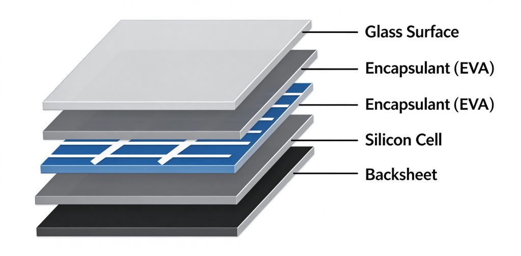
A typical crystalline‑silicon PV module adopts a multi‑layer laminated stack: front tempered glass, EVA (ethylene‑vinyl acetate) encapsulant layer, silicon solar cells, another EVA bonding layer, and composite TPT backsheet (PET substrate coated with PVF fluoropolymer films). The EVA polymer tightly bonds glass, cells and backsheet together, which creates the core technical barrier for component delamination.
Thermogravimetric tests under air atmosphere reveal two distinct weight‑loss stages for both EVA encapsulant and TPT backsheet:
- EVA thermal decomposition: The first stage occurs from 260 °C‑400 °C, corresponding to ester‑bond cleavage and release of acetic acid, contributing roughly 25 % mass loss. The second major decomposition stage runs from 400 °C‑525 °C for polyethylene‑chain degradation, with approximately 75 % weight loss. EVA can be fully decomposed without solid residues above 525 °C.
- TPT backsheet thermal decomposition: Two degradation peaks appear within 300‑550 °C. Around 80 % mass loss takes place between 300‑480 °C, and residual aromatic compounds leave about 8 % solid ash after full pyrolysis. Notably, direct heating of the fluorine‑containing TPT backsheet generates pungent, corrosive flue gas containing HF and fluorinated organics. Therefore pre‑removal of the backsheet before thermal processing greatly improves operational environmental performance.
Core Process Parameters of Optimized Thermal‑Treatment Recycling
Bench‑scale box‑furnace thermal experiments demonstrate that three critical factors dominate silicon‑wafer intactness: maximum thermal‑treatment temperature, heating rate, and whether the TPT backsheet is pre‑stripped. Holding time is fixed at 45 min to guarantee thorough polymer decomposition.
1. Treatment temperature
When the temperature is lower than 440 °C, EVA and backsheet polymers cannot be fully decomposed, and layered separation cannot be realized. 480 °C proves to be the optimal peak temperature. At this setting, organic encapsulants are fully decomposed, and we can retrieve complete front glass. If temperature rises further above 480 °C, accelerated polymer decomposition generates large‑volume instant gas, building internal pressure inside module laminates and causing cracking of silicon wafers.
2. Heating‑up rate
Heating rate directly affects gas‑escape behaviour and thermal‑stress distribution inside PV laminates.
- When heating rate is set at 20 °C·min⁻¹ (peak temperature 480 °C, 45 min holding): pre‑backsheet‑removed samples achieve near‑100 % silicon‑wafer intact rate; samples retaining original backsheet reach ~93 % wafer integrity.
- At heating rates below 20 °C·min⁻¹: wafer intact ratio rises with increasing heating speed.
- At heating rates higher than 20 °C·min⁻¹: rapid gas evolution creates chaotic internal thermal stress, leading to sharp drop in silicon‑wafer integrity.
3. Pre‑removal of TPT backsheet
TPT backsheet will shrink sharply under heating and produce mechanical stress that fractures silicon cells. Under identical temperature‑heating‑rate conditions, modules with backsheet pre‑stripped deliver far higher silicon‑wafer intactness. This pretreatment also eliminates most fluorine‑containing harmful fumes during thermal decomposition and simplifies flue‑gas purification work.
Material characterisation via SEM‑EDS confirms that after qualified thermal treatment, organic EVA is almost completely eliminated. Recovered silicon wafers retain silver front‑side grid‑line residues and aluminium back‑electrode components. Minor surface oxidation of aluminium electrode occurs under air atmosphere, which can be removed by follow‑up simple surface cleaning.
Advantages of Our Thermal‑Recycling Solution
✅ High silicon‑wafer intact yield: Far higher than conventional recycling approaches (traditional processes often deliver merely 60‑70 % intact rate). Complete silicon wafers can go for cell remanufacturing instead of being melted down into low‑grade silicon raw material, maximising material economic value. ✅ High‑quality co‑recovery: Intact tempered cover glass can be recycled and reused. Silver, aluminium and copper metallic fractions are preserved for subsequent metal extraction. ✅ Reduced secondary pollution: Pre‑removal of fluorinated TPT backsheet cuts hazardous flue‑gas output. Avoids large‑volume toxic organic solvents used in chemical dissolution workflows. ✅ Process robustness: Mature thermal‑treatment principle, easy‑to‑scale parameters, compatible for continuous industrial‑line transformation.
Application & Outlook
As global end‑of‑life PV waste volume grows year by year, high‑value component recycling is key to closing the circular‑economy loop for the whole photovoltaic supply chain. Our thermal‑delamination technology focuses on retrieving reusable whole silicon wafers rather than low‑value crushed materials. Combined with automated backsheet‑stripping pre‑treatment and standard flue‑gas treatment systems, this solution can serve waste‑PV‑module recycling plants across different regions.
Moving forward, we will further optimise energy consumption, explore semi‑continuous thermal‑processing equipment design, and cooperate with downstream silicon‑cell refurbishment enterprises to build a full‑chain solution from waste‑panel intake to regenerated‑silicon‑cell output.